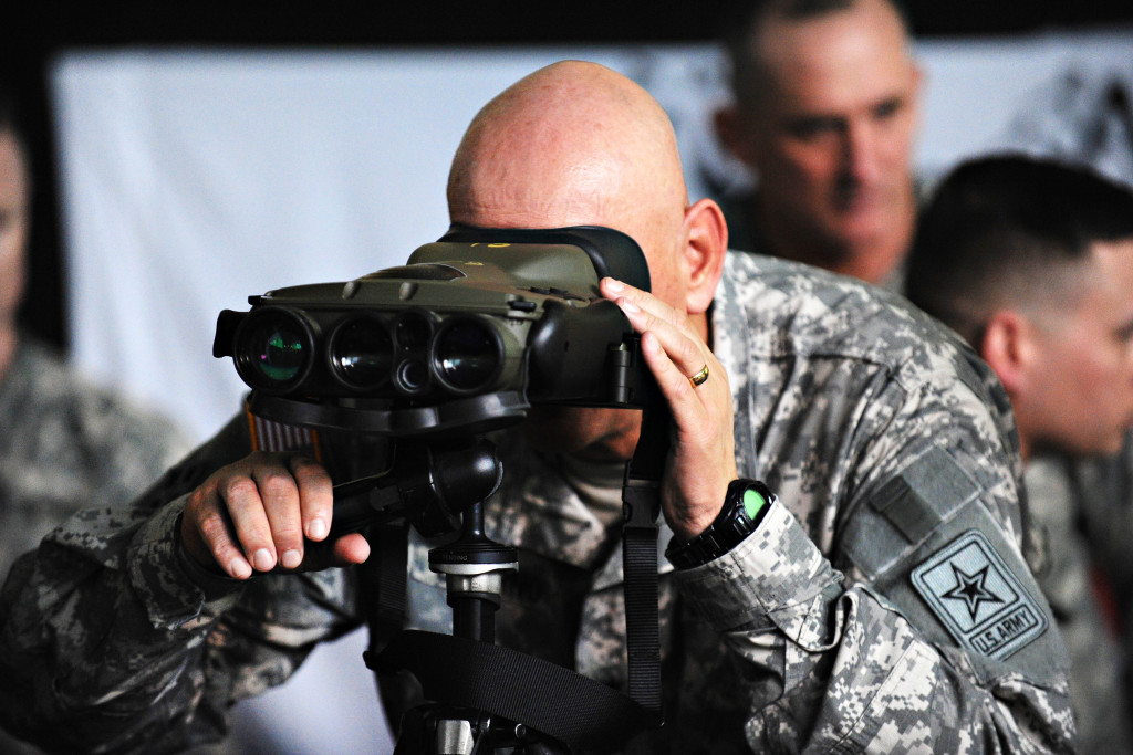
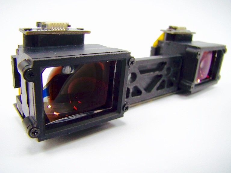
The Eagle Eye X is a high fidelity hd 1080p Color very high resolution dual Eye OLED binocular system catered to OEM or standalone high intensity viewing.
The system Incorporates 2 OLED Micro Displays with WUXGA, QWXGA or QXGA bright vivid OLED micro-displays. The unit is a very low power,
SWaP system with a standard HDMI video input. Traditional binocular microdisplay binocular viewers have low resolution and image distortion.
The Eagle Eye-X binocular color OLED micro-display viewers have fully adjustable Inter-pupillary distance and clear coated optics with adjustable diopter from -5 to +5
ocular diopter settings. All drivers and electronics are included..We utilize the highest Fidelity, robust 1920×1200 oled color micro displays.
Custom hd 1080p microdisplays for VR, AR or simulated military devices

The high grade system is extremely rugged and economical & can be customized to fit your requirements rapidly.


When looking into the Eagle Eye-X, the user is immersed with an extremely high resolution picture with fine precise details for increased situational awareness / crisp, rich 1920×1200 oled color microdisplays
The Eagle Eye-X system is ideal for:
-Multi sensor binocular viewer systems
-Low Light Level binocular viewers
-Virtual Reality systems
-OEM Custom imaging system packaging
-Long Range dual eye digital electronic binoculars
-Imaging systems where high resolution depth perception is required
-Wide area security and surveillance binocular system
-R&D, industrial and commercial imaging applications
Contact Mike@x20.org for pricing and additional details.

Previous, current and future SPI OLED, AMOLED and LCD micro displays and systems
CGA 320 x 200
QVGA 320 x 240
VGA 640 x 480
NTSC 720 x 480
WVGA 854 x 450
WVGA 800 x 480
PAL 768 x 576
SVGA 800 x 600
XGA 1024 x 768
N/A 1152 x 768
HD 720 1280 x 720
WXGA 1280 x 800
WXGA 1280 x 768
SXGA 1280 x 1024
N/A 1366 x 768
N/A 1440 x 960
SXGA+ 1400 x 1050
WSXGA 1680 x 1050
UXGA (2MP) 1600 x 1200
HD1080 1920 x 1080
WUXGA 1920 x 1200
QXGA (3MP) 2048 x 1536
WQXGA 2560 x 1600
QSXGA (5MP)
monocular (mono) and custom Oled embedded systems available for out of the box, or oem embedded integration projects/programs
Preliminary OLED data: Emissive, Color OLED on Silicon Format: 1920 x 1200 pixels Brightness Control 8 Levels Color Pixel Aspect Ratio: 9.6-micron Square Color Pixel Arrangement R, G, B, Vertical Stripe Fill Factor 71% Viewing Area 18.7 x 11.75 mm (22.1 mm diagonal (0.856”)) Size 26.4 x 17.5 x 4.72 mm (w x l x h) Gray Levels 256 levels per primary color Uniformity > 85% end-to-end uniformity Pixel Spatial Noise <5% (1 STD) Contrast Ratio >1,000:1 Pixel Response Linear with input video signal (using internal gamma LUT) Dimming Ratio >200:1 analog, >500:1 pwm, >50,000:1 total White Luminance (color display) >150 cd/m2 CIE White cie-x = 0.27 to 0.37, cie-y = 0.32 to 0.38 Video Modes WUXGA, HD1080, UXGA, 8-bit control of active window Progressive & Interlaced scan Horizontal (left/right) and vertical (up/down) scan control Frame/field sequential stereo support Horizontal and vertical image shift by up to 24 pixels Variable row duty rate control Video Interface Serialized LVDS, 24b Digital RGB (8 twisted line pairs) Refresh Rate 60Hz Video Source Clock 220 MHz max LVDS Clock 442 MHz max LVDS Data Rate 883 Mbps Control Interface 3.3V to 5V I 2 C serial interface Power Consumption <350 mW typical @ 150cd/m2 (1W max) Power Supply VAN (analog & array) 5VDC ±5% (150 mA maximum) VDD (logic & I/Os) 1.8VDC ±5% (30 mA maximum) VPG -1.5VDC ±5% (1 mA maximum) Operating ambient temperature -45 to +70°C Storage temperature -55to +90°C Humidity 85%RH non condensing
Size, power, contrast and color space advantages make OLED microdisplays a perfect fit for near-eye applications. Advances in subpixel patterning and the development of stacked OLEDs promise to extend color space and battery life
Mobile personal electronics and wearables have become immensely popular around the globe, and this has given rise to a new dilemma. Screen content has grown, mainly from multimedia applications, resulting in increased display pixel count. The initial black and white character displays in early mobile phones have evolved into full-HD (FHD), full-color video displays and beyond. Even the screen diagonals have become larger: There is only a single smartphone product on the market featuring FHD active-matrix organic light-emitting diodes (AM-OLEDs) at <5 in., but many at larger screen formats. Besides the technical issues of achieving high pixel density, most mobile display screen sizes are bigger than 5 in., and, depending on the geographic region, even greater than 7 in.
Size, power, contrast and color space advantages make OLED microdisplays a perfect fit for near-eye applications. Advances in subpixel patterning and the development of stacked OLEDs promise to extend color space and battery life.
Mobile personal electronics and wearables have become immensely popular around the globe, and this has given rise to a new dilemma. Screen content has grown, mainly from multimedia applications, resulting in increased display pixel count. The initial black and white character displays in early mobile phones have evolved into full-HD (FHD), full-color video displays and beyond. Even the screen diagonals have become larger: There is only a single smartphone product on the market featuring FHD active-matrix organic light-emitting diodes (AM-OLEDs) at <5 in.but many at larger screen formats. Besides the technical issues of achieving high pixel density, most mobile display screen sizes are bigger than 5 in., and, depending on the geographic region, even greater than 7 in, content will continue to increase, and will continue to do so, especially with upcoming virtual- and augmented-reality applications. Yet users generally prefer to keep their smartphones “mobile” and thus need to limit the size of the device, hence the display screen size. Fortunately, set manufacturers have managed to keep the device size very close to the display size, and do not require much extra space beyond it.
There are two general ways to address the balancing act of mobile screen content versus size: The first is to create a physically larger screen size at a reduced form-factor. This would be a move away from rigid planar screens; for example, they could be made rollable, to fit into smaller spaces.
Another option is to move from direct view toward projection, by generating a larger screen perception toward the user by either real or virtual optical magnification. The latter one is the opportunity for microdisplays in general since, due to their unprecedented pixel density, they are able to generate high-resolution virtual images with a large viewing angle at a very small device footprint.
All microdisplay technologies on the market comprise an image-creating pixel modulation, but only the emissive ones (for example, OLED and LED) feature the image and light source in a single device, and therefore do not require an external light source. This minimizes system size and power consumption, while providing exceptional contrast and color space. Organic light-emitting diodes (OLEDs) are made from ultra-thin organic semiconducting layers, which light up when they are connected to voltage (charge carriers become injected and luminance mainly is proportional to the forward current). The major layers comprise several organic materials in sequence (for example, charge transport, blocking and emission layers — each with a thickness of several nanometers), which are inserted between an anode and a cathode. OLED microdisplays cover the major portion of emissive microdisplays on the market today as they are well-suited for extremely small form-factor and low-power consuming optical engines. They are the first choice for mobile.
Near-to-eye applications growing
The growing market for wearable devices requires a high number of small and lightweight displays for different applications in sports, medicine or at work. The global market for near eye microdisplays expanded in the 1990s, mainly due to rising demand for projection applications, specifically front projectors and rear-projection TV (RPTV). Whereas RPTV significantly declined after 2005, other applications have arrived, mainly in near-to-eye (NTE) displays, HMD.
Due to the size, power, contrast and color-space advantages, NTE applications represent the largest opportunity for OLED microdisplays. This relates to both personal viewers (PV) and electronic viewfinders (EVF). As of today, there are three main markets for near-eye OLED micro-displays. The consumer market encompasses video and virtual-reality (VR) glasses and EVF; industrial covers augmented-reality (AR) smart glasses for logistics;military/defense market targets AR helmets for pilots
PV are either see-through data glasses used for mixed- and augmented reality (AR) applications, or non-see-through/immersive video glasses used for entertainment or virtual reality (VR) applications in gaming, training or entertainment. Due to their emissive nature OLED microdisplays are specifically suited for see-through/AR smart glasses, since they prevent a virtual gray-shaded monitor-like perception inside the user’s field of view, which is caused by the insufficient backlight suppression of non-emissive microdisplays. The market is expected to grow significantly in PV applications, with major expected growth for see-through data glasses. The market analysis firm Tractica estimates that smart augmented-reality glass shipments will surpass 12 million units between 2015 and 2020, while more than 200 million virtual reality head-mounted displays will be sold by 202. Consumer and enterprise segments will both drive sector growth, with additional sizable markets for industrial and sports applications.
Electronic viewfinders in cameras
cameras — mostly high-end models that adopt OLED microdisplays for the EVF. In 2012 microdisplay unit shipments for electronic viewfinders were 4 million, with 7 million in 2013, according to a report from Insight Media. The market should continue to grow significantly, with an expected shift of EVFs from primarily high-end cameras toward midrange consumer devices. There is also a market in EVF for digital video cameras and camcorders; however, this is expected to decline driven by a shrinking camcorder market and the use of direct view panels in high-end viewfinders.
Micro-projection in sight
Projection is still the major application of microdisplays. Due to limited luminance and luminous flux capabilities of OLED, the use of OLED microdisplays for front-projection has been limited. However, in 2010 the HYPOLED project demonstrated OLED microdisplays in micro-projection, though full-color projection had only been feasible using a three-panel approach comprising three monochrome subpanels (R, G, B) and optical color-combining. Red and green monochrome micro-projectors worked quite well at limited luminous flux, but displays had to be driven at around 10000 nits (a nit is a unit of luminance equivalent to one candela per square meter). This significantly affected OLED lifetime.
OLED-on-silicon
The prominent emissive microdisplay technology on the market is OLED-on-silicon. A single-crystalline silicon CMOS chip provides the active-matrix circuitry to address and drive the millions of individual pixels. Since the silicon substrate itself is intransparent in the visible spectrum, a top-emission OLED setup is required
LED microdisplays
The term “microLED” refers to a variety of approaches that combine III/V-based inorganic LEDs with a silicon backplane, either monolithically or hybrid.
Due to recent promising activities of III/V LED or RF/power component manufacturers to transfer III/V processes onto silicon-compatible 8-in. equipment for cost reasons, monolithic silicon-III/V hetero-integration — GaN-on-Silicon, for example — could become a competitive technology for emissive microdisplays in about 10 years. Cost may be comparable to OLED-on-silicon over the long run, but some characteristics such as lifetime, high-temperature performance, spectral width and switching speed, could prove superior
Subpixel patterning
To address the challenges of high luminance operation, improvements are required in the current color generation approach by white OLED emission and absorption-filter color separation. To overcome this luminance/power-inefficient approach, monochrome subpixels featuring individual spectral emitters in red, green and blue could be a better alternative. That would directly benefit current and power efficiency, thus lifetime, and color space. For direct-view active-matrix organic light-emitting diode (AMOLED) displays, such an approach has been in large volume production at Samsung Display by shadow-masking or “fine metal masking,” but those and other patterning approaches currently exhibit a lower feature size limit at about 50 µm. The OLED microdisplay feature sizes in the range of 5 µm or below have not been shown in a productive micropatterning process so far.
Microdisplay application
the high-resolution photolithography commonly adopted in microelectronics cannot be applied to OLED easily, since their photochemistry materials are going to affect the organic semiconductor materials due to their hydrophilic behavior. There are potential options to overcome this issue; for example, one way involves the effect of chemical orthogonality to a specifically adapted photochemistry for organic semiconductors. Alternative approaches could involve micro-shadow-masking, flash mask transfer lithography or electron beam patterning,
Yet any of those have to prove manufacturing feasibility for micropatterning for OLED microdisplays.
Future forward: OLED-on-silicon
There is a trend toward high-brightness, and improved current and power efficiency, as can be seen in the development of stacked OLED devices. This will be accompanied by a monochrome subpixel micropatterning approach, which will extend color space and battery life for mobile applications. That’s always an important driving force, which may lead to new low-power microdisplay architectures. Specifically the bidirectional OLED microdisplay feature provides great opportunity for OLED microdisplay applications well beyond near-to-eye, for example, in optical inspection and optoelectronic sensors.


